Physicists Use Food Wrap in Nanoelectronics Breakthrough
In the realm of femtosecond lasers and gravitational waves, everyday items like tape, glue, and glass or plastic containers are essential. Now, food wrap has been added to the toolkit of microelectronics specialists.
Scientists and industry have long worked with materials just a few atoms thick. These materials are considered two-dimensional, and their properties differ significantly from bulk materials.
In laboratory settings, tape is commonly used to separate layers of material. This method produces graphene, a layer of carbon just one atom thick. While effective, it has its drawbacks. The material can crack, and it is often removed from the tape in tiny flakes that are too small for most devices. Additionally, they must be cleaned of adhesive.
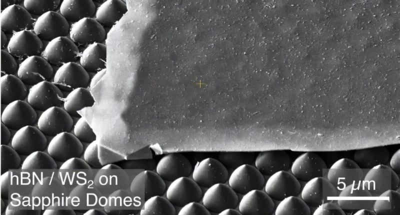
Physicists have developed a method to transfer ultrathin materials onto textured surfaces without damaging either the transferred layer or the surface. Food wrap made from low-density linear polyethylene (LDPE) is ideal for this task. Researchers reported this in an article for ACS Nano.
Read this article in full and everything else in Telegram, ad-free
Open in TelegramThanks, I just want to finish reading here
In their experiment, they transferred a monolayer of WS2 from a silicon oxide substrate to another silicon oxide layer. They created a stamp made from a drop of superglue covered with food wrap. The stamp was brought into contact with WS2 heated to 70° C, and then the system was heated to 140° C to form a strong bond. At this temperature, LDPE melts and captures the sample.
Next, the stamp was moved to another substrate and heated to 150 °C. This further altered the properties of LDPE, reducing the polymer's viscosity. At this stage, the researchers slid the stamp aside, leaving a monolayer of WS2 with residual LDPE on the surface. They removed it using oleic acid, orthoxylene, and isopropyl alcohol. The same process was nearly repeated for transferring a heterostructure with hexagonal boron nitride, but the temperature and solvents used to remove the film residues were adjusted.
“The discovery of the possibility of using food wrap for this application happened completely by accident. We were trying to reproduce results from a research group in Japan, but it turned out that the food wrap used in Europe is made from a different polymer. We noticed that the polymer used here melts at 120 °C, while theirs does not. This property turned out to be a decisive factor for the successful transfer of the 2D material: we could simply melt the food wrap over the material for it to adhere,” said Professor Jorik van de Groep.
Scientists believe that this new technique has great potential. It not only allows for the transfer of fragile materials but also enhances their emission characteristics. This paves the way for industrial production of transistors and ultrathin optical elements based on two-dimensional materials.